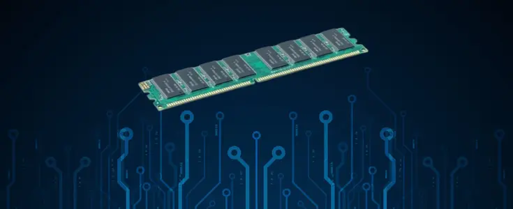
RAM

Random-access memory (commonly known by its acronym RAM) refers to data storage formats and equipment that allow the stored data to be accessed in any order — that is, at random, not just in sequence. In contrast, other types of memory devices (such as magnetic tapes, disks, and drums) can access data on the storage medium only in a predetermined order due to constraints in their mechanical design.

Generally, RAM in a computer is considered main memory (or primary storage): the working area used for displaying and manipulating data. This type of RAM is usually in the form of integrated circuits (IC). These are commonly called memory sticks or RAM sticks because they are manufactured as small circuit boards with plastic packaging and are about the size of a few sticks of gum. Most personal computers have slots for adding and replacing memory chips.

RAM is typically erased when a computer is shut down, though some RAM chips maintain data indefinitely without electrical power. Technically, RAM devices are not limited to memory chips, and random-access memory as a storage format is not limited to use as working memory. In a broad sense, modern storage devices for long-term or secondary storage, including magnetic media and laser-readable CDs and DVDs, are forms of random-access memory.

Look up RAM, random access memory in Wiktionary, the free dictionary.Most RAM can be both written to and read from, so “RAM” is often used interchangeably with “read-write memory.” In this sense, RAM is the opposite of read-only memory (ROM). Strictly speaking, however, “RAM” and “ROM” are not mutually exclusive designations because “RAM” refers only to the method of accessing stored data, not whether data can be written
 

DIP

In microelectronics, a dual in-line package (DIP), sometimes called a DIL package, is an electronic device package with a rectangular housing and two parallel rows of electrical connecting pins, usually protruding from the longer sides of the package and bent downward. A DIP is usually referred to as a DIPn, where n is the total number of pins.

DIPs may be used for integrated circuits (ICs, “chips”), like microprocessors, or for arrays of discrete components such as resistors or toggle switches. They can be mounted on a printed circuit board (PCB) either directly using through-hole technology, or using inexpensive sockets to allow for easy replacement of the device. A typical DIP may be a microcircuit package with two rows of seven vertical leads (i.e., a DIP14).

The most common DIPs have an inter-lead spacing (lead pitch) of 0.1″ (2.54 mm) and a row spacing of either 0.3″ (7.62 mm) or 0.6″ (15.24 mm). Typical pin counts are 8 or any even number from 14 to 24 (less common 28) for 0.3″ packages, and 24, 28, 32 or 40 (less common 36, 48 or 52) for 0.6″ packages. JEDEC-standards also specify less common packages with a row spacing of 0.4″ (10.16 mm), or 0.9″ (22.86 mm) with a pin-count of up to 64. Other standardized variants include a lead pitch of 0.07″ (1.778 mm) at a row spacing of 0.3″, 0.6″ or 0.75″.

Several DIP variants exist, mostly distinguished by packaging material:

Ceramic Dual In-line Package (CERDIP)
Plastic Dual In-line Package (PDIP)
Shrink Plastic Dual In-line Package (SPDIP) – A shrink version of the PDIP with a 0.07″ (1.778 mm) lead pitch
DIPs were the mainstream of the microelectronics industry in the 1970s and 80s. Their use has subsided in recent years due to the emerging new surface-mount technology (SMT) packages such as PLCC and SOIC.

For programmable devices like EPROMs and GALs, DIPs remained popular for many years due to their easy handling with external programming circuitry. However, with In-System Programming (ISP) technology now state of the art, this advantage of DIPs is rapidly losing importance as well.
 

SIMM

A SIMM, or single in-line memory module, is a type of memory module used for random access memory in personal computers. It differs from a DIMM (the most predominant form of memory module today) in that the contacts on a SIMM are redundant on both sides of the module.

Most early PC motherboards (8088 based PCs and XTs) used socketed DIP chips. With the introduction of 80286 based PC/ATs, which could use larger amounts of memory, memory modules evolved from the need of saving motherboard space and to ease memory expansion. Instead of plugging in 8 or 9 single DRAM DIP chips, only one additional memory module was needed to increase the memory of the computer. A few 80286-based computers used (often non-standard) memory modules like SIPP memory (single in-line pin package). SIPP’s 30 pins often bent or broke during installation, which is why they were quickly replaced by SIMMs which used contact plates rather than pins.

The first variant of SIMMs has 30 pins and provides 8 bits of data (9 bits in parity versions).

The second variant of SIMMs—also called PS/2 after the IBM line of computers in which it was first used—has 72 pins and provides 32 bits of data (36 bits in parity versions).

Macintosh IIx and Macintosh IIfx has non-standard 64-pin SIMMs.

Due to the differing data bus widths of the memory modules and some processors, sometimes several modules must be installed in pairs to fill a memory bank. For instance, on 80386 or 80486 systems (data bus width of 32 bits), either four 30-pin SIMMs or one 72-pin SIMM are required for one memory bank. On Pentium systems (data bus width of 64 bits), two 72-pin SIMMs are required.

To install a SIMM, the module must be placed in the socket at an angle, then rotated (angled) into position. To remove one, the two metal or plastic clips at each end must be pulled to the side, then the chip must be tilted back and pulled out.

RAM technologies used on SIMMs include EDO and FPM.

SIMM is standardised under JEDEC JESD-21C standard.


SIMM 32

SIMM 72 (EDO – PS/2)

EDO DRAM is similar to Fast Page Mode DRAM with the additional feature that a new access cycle can be started while keeping the data output of the previous cycle active. This allows a certain amount of overlap in operation (pipelining), allowing somewhat improved speed. It was 5% faster than Fast Page Mode DRAM, which it began to replace in 1993.

Single-cycle EDO has the ability to carry out a complete memory transaction in one clock cycle. Otherwise, each sequential RAM access within the same page takes two clock cycles instead of three, once the page has been selected. EDO’s speed and capabilities allowed it to somewhat replace the then-slow L2 caches of PCs. It created an opportunity to reduce the immense performance loss associated with a lack of L2 cache, while making systems cheaper to build. This was also good for notebooks due to difficulties with their limited form factor, and battery life limitations. Performance was still lost though, and an EDO system with L2 cache was tangibly faster than the older FPM/L2 combination.

Single-cycle EDO DRAM became very popular on video cards towards the end of the 1990s. It was very low cost, yet nearly as efficient for performance as the far more costly VRAM.

EDO was sometimes referred to as Hyper Page Mode.


Fast Page Mode DRAM (FPM) (for explain purpose only)
Fast page mode DRAM is also called FPM DRAM, Page mode DRAM, Fast page mode memory, or Page mode memory.

In page mode, a row of the DRAM can be kept “open”, so that successive reads or writes within the row do not suffer the delay of precharge and accessing the row. This increases the performance of the system when reading or writing bursts of data.

Static column is a variant of page mode in which the column address does not need to be strobed in.

Nibble mode is another variant in which four sequential locations within the row can be accessed.

DRAM (for explain purpose only)
Dynamic random access memory (DRAM) is a type of random access memory that stores each bit of data in a separate capacitor. As real-world capacitors are not ideal and hence leak electrons, the information eventually fades unless the capacitor charge is refreshed periodically. Because of this refresh requirement, it is a dynamic memory as opposed to SRAM and other static memory. Its advantage over SRAM is its structural simplicity: only one transistor and a capacitor are required per bit, compared to six transistors in SRAM. This allows DRAM to reach very high density. Since DRAM loses its data when the power supply is removed, it is in the class of volatile memory devices
 

SIMM 32 to 72 adapter

DIMM

A DIMM, or dual in-line memory module comprises a series of random access memory integrated circuits. These modules are mounted on a printed circuit board and designed for use in personal computers. DIMMs began to replace SIMMs (single in-line memory modules) as the predominant type of memory module as Intel’s Pentium processors began to control the market.

The main difference between SIMMs and DIMMs is that SIMMs have a 32-bit data path, while DIMMs have a 64-bit data path. Since Intel’s Pentium has a 64-bit bus width, it required SIMMs installed in matched pairs in order to use them. The processor would then access the two SIMMs simultaneously. DIMMs were introduced to eliminate this inefficiency. Another difference is that DIMMs have separate electrical contacts on each side of the module, while the contacts on SIMMs on both sides are redundant.

The most common types of DIMMs are:

72-pin-DIMMs, used for SO-DIMM
144-pin-DIMMs, used for SO-DIMM
168-pin-DIMMs, used for FPM, EDO and SDRAM
184-pin-DIMMs, used for DDR SDRAM
240-pin-DIMMs, used for DDR2 SDRAM
There are 2 notches on the bottom edge of 168-pin-DIMMs, and the location of each notch determines a particular feature of the module.

The first notch is DRAM key position. It represents RFU, buffered, and unbuffered.
The second notch is voltage key position. It represents 5.0V, 3.3V, and Reserved.
The upper DIMM in the photo is an unbuffered 3.3V 168-pin DIMM.
A DIMM’s capacity and timing parameters may be identified with SPD (Serial Presence Detect), an additional chip which contains information about the module type.

ECC DIMM RAM has additional Error Correcting Code housed in the DIMM package.


SD-RAM (DIMM)

SDR SDRAM is Single Data Rate synchronous dynamic random access memory, a type of computer memory. The term is used to contrast with Double Data Rate SDRAM, or DDR SDRAM, but since single data rate SDRAM was the only sort available when SDRAM was introduced, is simply called “SDRAM”, rather than “SDR SDRAM”.

While other forms of DRAM have an asynchronous interface, meaning that it reacts immediately to changes in its control inputs, SDRAM has a synchronous interface, meaning that it waits for a clock pulse before responding to its control inputs- it synchonizes with the computer’s system bus, and thus with the processor. The clock is used to drive an internal finite state machine that can pipeline incoming commands. This allows the chip to have a more complex pattern of operation than plain DRAM.

Pipelining means that the chip can accept a new command before it has finished processing the previous one. In a pipelined write, the write command can be immediately followed by another command without waiting for the data to be written to the memory array. In a pipelined read, the requested data appears a fixed number of clock pulses after the read command. It is not necessary to wait for the data to appear before sending the next command. This delay is called the latency, and is an important parameter to be considered when purchasing SDRAM for your computer.

SDRAM for PCs is rated for its potential maximum clock rate. Speeds included PC66, PC100, and PC133, representing 66, 100 and 133 megahertz. There were additional unofficial speeds for enthusiast SDRAM parts, such as PC150, for 150 MHz. SDRAM comes in 168-pin DIMMs for desktops, or 144-pin SODIMMs mainly used in laptops, while DDR SDRAM comes in 184-pin DIMMs, and DDR2 uses a 240-pin configuration.

SDRAM was introduced in 1997, and by 2000 had replaced all other types of DRAM in modern computers, because of its greater speed, and much lower latency.

SDRAM is also available in registered memory varieties, for systems that need greater scalability.

Currently, 168-pin SDRAM type is not used in new PC systems, and PCs come with DDR or DDR2 SDRAM, with DDR2 quickly phasing out DDR.


SO-DIMM

A SO-DIMM, or small outline dual in-line memory module, is a type of computer memory integrated circuit.

SO-DIMMs are a smaller alternative to a DIMM, being roughly half the size of regular DIMMs. As a result SO-DIMMs are mainly utilised in laptops, small footprint PCs (such as those with a Mini-ITX motherboard) and high-end upgradable office printers.

SO-DIMMs have 100 pins (supporting 32-bit data transfer) or 144 or 200 pins (both supporting 64-bit data transfer). This compares to regular DIMMs that have 168 pins and support 64-bit data transfer.

The different types of SO-DIMMs can be recognized at a glance by the distinctive notches used to “key” them for different applications: 100-pin SO-DIMMs have two notches, 144-pin SO-DIMMs have a single notch near (but not at) the center, and 200-pin SO-DIMMs have a single notch nearer to one side.

DDR-RAM (DIMM)


DDR memory (front and back shown) has 184 pins and one notch.DDR SDRAM or double-data-rate synchronous dynamic random access memory is a type of memory integrated circuit used in computers. It achieves greater bandwidth than ordinary SDRAM by transferring data on both the rising and falling edges of the clock signal (double pumped). This effectively nearly doubles the transfer rate without increasing the frequency of the front side bus. Thus a 100 MHz DDR system has an effective clock rate of 200 MHz when compared to equivalent SDR SDRAM, the “SDR” being a retrospective designation.

With data being transferred 8 bytes at a time DDR RAM gives a transfer rate of (memory bus clock rate) × 2 (for dual rate) × 8 (number of bytes transferred). Thus with a bus frequency of 100 MHz, DDR-SDRAM gives a max transfer rate of 1600 MB/s.

JEDEC has set standards for speeds of DDR SDRAM, divided into two parts: The first specification is for memory chips and the second is for memory modules.


Chip specification
DDR-200: DDR-SDRAM memory chips specified to run at 100 MHz
DDR-266: DDR-SDRAM memory chips specified to run at 133 MHz
DDR-333: DDR-SDRAM memory chips specified to run at 166 MHz
DDR-400: DDR-SDRAM memory chips specified to run at 200 MHz

Stick/module specification
PC-1600: DDR-SDRAM memory module specified to run at 100 MHz using DDR-200 chips, 1.600 GByte/s bandwidth per channel.
PC-2100: DDR-SDRAM memory module specified to run at 133 MHz using DDR-266 chips, 2.133 GByte/s bandwidth per channel
PC-2700: DDR-SDRAM memory module specified to run at 166 MHz using DDR-333 chips, 2.667 GByte/s bandwidth per channel
PC-3200: DDR-SDRAM memory module specified to run at 200 MHz using DDR-400 chips, 3.200 GByte/s bandwidth per channel
Note: All RAM speeds in-between or above these listed specifications are not standardized by JEDEC — most often they are simply manufacturer optimizations using higher-tolerance chips.

The package sizes in which DDR SDRAM is manufactured are also standardised by JEDEC.

There is no architectural difference between DDR SDRAM designed for different clock frequencies, e.g. PC-1600 (designed to run at 100 MHz) and PC-2100 (designed to run at 133 MHz). The number simply designates the speed that the chip is guaranteed to run at. Hence you can run DDR SDRAM at lower clock speeds than it was made for (underclocking) or higher clock speeds than it was made for (overclocking). Note that overclocking should only be done by those that know what they are doing (see overclocking for details on why).

DDR SDRAM DIMMs have 184 pins (as opposed to 168 pins on SDR SDRAM, or, 240 pins on DDR-2), and can be differentiated from SDRAM DIMMs by the number of notches (DDR SDRAM has one, SDR SDRAM has two). DDR operates at a voltage of 2.5 V, compared to 3.3 V for SDR SDRAM. This can significantly reduce power usage.

Some new chipsets use these memory types in dual or even quad channel configurations, which doubles or quadruples the effective bandwidth. In the dual-channel configuration it is recommended to use a matched pair of memory modules to optimize performance. The modules in a pair have the same size, speed, and latency timings, enabling the chipset to interleave accesses with maximum efficiency.
 

RD-RAM (RIMM)

The Direct RDRAM features an architecture and a protocol designed to achieve high bandwidth. The Rambus channel architecture has a single-device upgrade granularity, offering engineers the ability to balance performance requirements against system capacity and component count. The narrow, high-performance channel also offers performance and capacity scalability through the use of multiple channels in parallel. In addition, the validation program created by Intel and Rambus promotes system stability by ensuring that devices and modules conform to published specifications. Although RDRAMs have a low pin count, a single device is capable of providing up to 1.6 GB/s bandwidth. Memory systems that use RIMMs (Rambus Inline Memory Modules), also known as RDRAM modules, employ a narrow, uniform-impedance transmission line, the Rambus Channel, to connect the memory controller to a set of RIMMs. Low pin count and uniform interconnection topology allow easy routing and reduction of pin count on the memory controller. While a single channel is capable of supplying 1.6 GB/s of bandwidth, multiple channels can be used in parallel to increase this number. Systems that use, for example, the Intel 840 chipset, have two parallel Rambus channels, and are able to handle up to 3.2 GB/s.

Providing high bandwidth from a single device also allows memory systems to be constructed from small numbers of RDRAMs. The Sony PlayStation 2 uses two RDRAM channels, each with a single RDRAM stick, to achieve a total of 3.2 GB/s memory bandwidth.

While RDRAM technology was designed to be cheaper to implement on the system level, the RIMM sticks themselves were not easy to manufacture in the beginning. Similar to how the Pentium Pro CPU could not be tested until both dies were integrated into the final package, the RIMM sticks needed to be completely assembled before testing could be performed. This created the scenario where if just one of the RDRAM chips was faulty, the entire stick had to be thrown away.

Early implementations suffered from much higher memory latency when compared to contemporary SDR SDRAM and DDR SDRAM designs, making SDR SDRAM or DDR SDRAM a better choice. Latency became worse as additional RIMM’s were added to the system, further hurting performance. Nintendo 64’s implementation was regarded as a very high latency memory subsystem.

Later designs mitigated the latency issue to the point where it was mostly competitive with DDR SDRAM, but by then Rambus had largely alienated hardware manufacturers due to its litigious nature. Consumer sentiment turned against Rambus in the same manner, and also because of RDRAM’s substantially higher price compared to other memory types. As of 2004, Intel had essentially abandoned RDRAM entirely, with all new products using DDR SDRAM or DDR2 SDRAM.

RDRAM memory sticks are available in a number of different speeds. Quite fittingly, PC800 has an 800MHz data rate using a 400MHz clock rate, PC1066 has a 1066MHz data rate using a 533MHz clock rate, etc. This is best described in Intel’s Developer UPDATE Magazine June 2002 article “Mainstream PC Memory Architectures for the Intel Pentium 4 Processor”. This use of Double Data Rate technology was included in RAMBUS’ patent portfolio, after being discussed openly in JEDEC meetings. RAMBUS used the patent to file several lawsuits against DDR SDRAM manufacturers. While a few companies settled, others challenged the lawsuit, and ownership of said intellectual property was eventually denied.


0 0 votes
Article Rating
Subscribe
Notify of
guest

This site uses Akismet to reduce spam. Learn how your comment data is processed.

0 Comments
Inline Feedbacks
View all comments