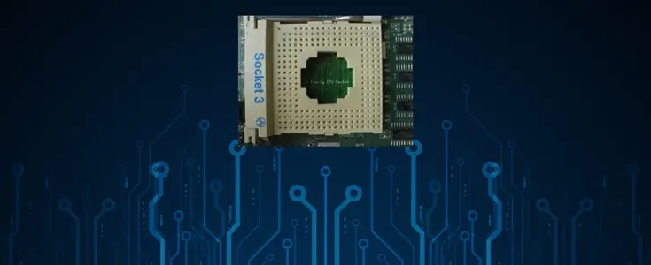
Intel's Socket 3 was a type of CPU socket into which various x86 microprocessors were inserted. It was commonly found alongside a secondary socket designed for a math coprocessor chip, in this case the 487. Socket 3 resulted from Intel's creation of…
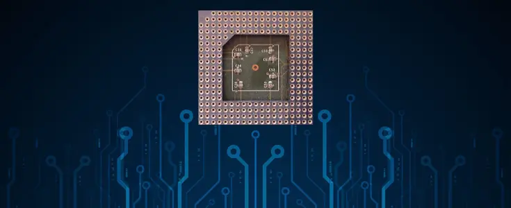
Socket 2 was one of the series of standard sockets into which various x86 microprocessors were plugged. It was an updated Socket 1 with added support for Pentium Overdrive processors.
It was a 238 pin LIF/ZIF PGA (19×19) socket suitable for the 5v,…
PGA 168 (Pin Grid Array) refers to a 168-pin CPU socket standard, primarily used for Intel 80486, Intel i960, and Cyrix/IBM Blue Lightning processors from the early-to-mid 1990s. These, often ceramic, chips feature a pin grid with spacing. They are…
Socket 1 was the second of a series of standard sockets created by Intel into which various x86 microprocessors were plugged. It was an upgrade to Intel's first standard PGA socket and the first with an official designation. Socket 1 was intended as a…
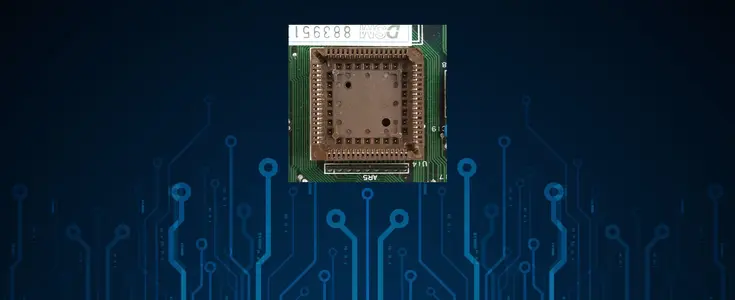
A plastic-leaded chip carrier (PLCC) has a rectangular plastic housing. It is a reduced cost evolution of the ceramic leadless chip carrier (CLCC).
A premolded PLCC was originally released in 1976, but did not see much market adoption. Texas Instruments…
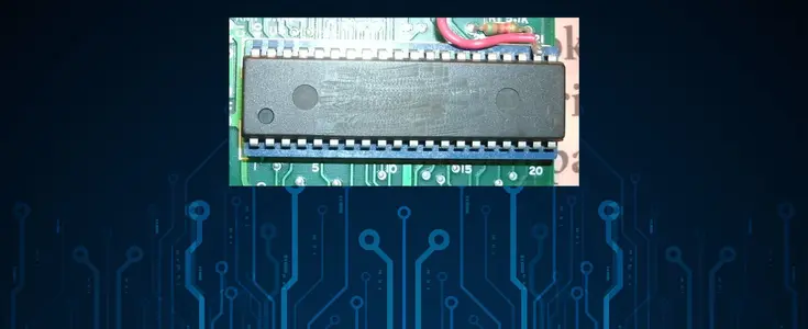
The 8086 (also called iAPX 86) is a 16-bit microprocessor chip designed by Intel between early 1976 and June 8, 1978, when it was released. The Intel 8088, released July 1, 1979, is a slightly modified chip with an external 8-bit data bus (allowing the…